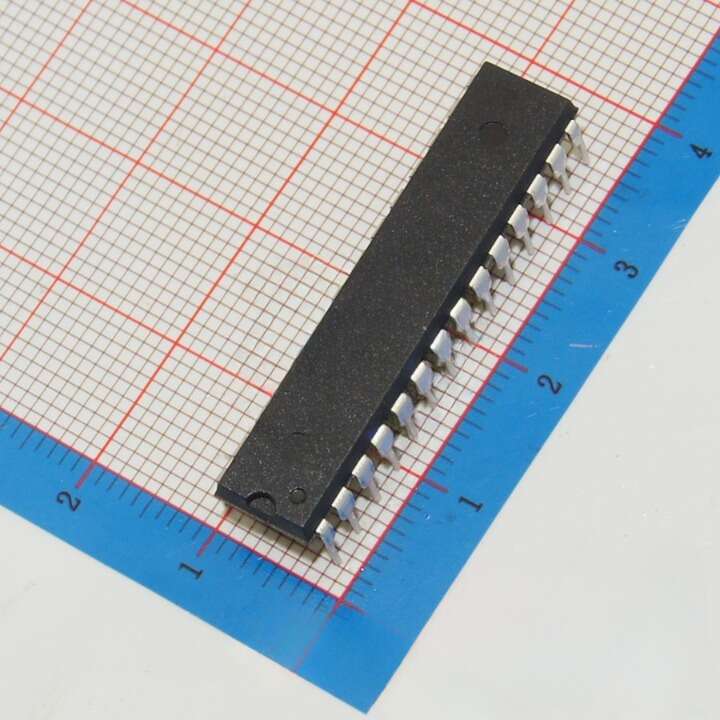
ATMEGA8A-PU 8KB 2.7V~5.5V AVR 1KB 16MHz FLASH 23 DIP-28 AVR Microcontroller Unit
EGP 160
See other suppliers →Description
Microcontroller from Atmel AVR 28-leg DIP case. Voltage supply ranges from 2.7 V to 5.5 V, frequency up to 16 MHz, has 8 KB Flash, 1 KB RAM, and 512 B of EEPROM. Specifications: Product Attribute Attribute Value Product Category: 8-bit Microcontrollers – MCU Core: AVR Program Memory Size: 8 kB Data RAM Size: 1 kB Package/Case: PDIP-28 Maximum Clock Frequency: 16 MHz ADC Resolution: 10 bit Number of I/Os: 23 I/O Supply Voltage – Min: 2.7 V Supply Voltage – Max: 5.5 V Mounting Style: Through Hole Data Bus Width: 8 bit Minimum Operating Temperature: – 40 C Maximum Operating Temperature: + 85 C Series: ATmega8A Data RAM Type: SRAM Data ROM Size: 512 B Data ROM Type: EEPROM Interface Type: SPI, TWI, USART Number of ADC Channels: 6 Channel Number of Timers/Counters: 3 Timer Program Memory Type: Flash Pin Configurations ATMEGA8 Pin Configuration Pin No. Pin name Description Alternate Function 1 PC6 (RESET) Pin6 of PORTC Pin by default is used as RESET pin. If the RSTDISBL Fuse is programmed, PC6 can be used as an I/O pin. (Pulled HIGH to RESET controller) 2 PD0 (RXD) Pin0 of PORTD RXD (USART Input Pin) USART Serial Communication Interface [Can be used for programming] 3 PD1 (TXD) Pin1 of PORTD TXD (USART Output Pin) USART Serial Communication Interface [Can be used for programming] INT2( External Interrupt 2 Input) 4 PD2 (INT0) Pin2 of PORTD External Interrupt INT0 5 PD3 (INT1) Pin3 of PORTD External Interrupt INT1 6 PD4 (XCK/T0) Pin4 of PORTD T0( Timer0 External Counter Input) XCK ( USART External Clock I/O) 7 VCC 8 GND 9 PB6 (XTAL1/TOSC1) Pin6 of PORTB XTAL1 (Chip Clock Oscillator pin 1 or External clock input) TOSC1 (Timer Oscillator pin 1) 10 PB7 (XTAL2/TOSC2) Pin7 of PORTB XTAL2 (Chip Clock Oscillator pin 2) TOSC2 (Timer Oscillator pin 2) 11 PD5 (T1) Pin5 of PORTD T1(Timer1 External Counter Input) 12 PD6 (AIN0) Pin6 of PORTD AIN0(Analog Comparator Positive I/P) 13 PD7 (AIN1) Pin7 of PORTD AIN1(Analog Comparator Negative I/P) 14 PB0 (ICP1) Pin0 of PORTB ICP1(Timer/Counter1 Input Capture Pin) 15 PB1 (OC1A) Pin1 of PORTB OC1A (Timer/Counter1 Output Compare Match A Output) 16 PB2 (SS/OC1B) Pin2 of PORTB SS (SPI Slave Select Input). This pin is low when controller acts as slave. [Serial Peripheral Interface (SPI) for programming] OC1B (Timer/Counter1 Output Compare Match B Output) 17 PB3 (MOSI/OC2) Pin3 of PORTB MOSI (Master Output Slave Input). When controller acts as slave, the data is received by this pin. [Serial Peripheral Interface (SPI) for programming] OC2 (Timer/Counter2 Output Compare Match Output) 18 PB4 (MISO) Pin4 of PORTB MISO (Master Input Slave Output). When controller acts as slave, the data is sent to master by this controller through this pin. [Serial Peripheral Interface (SPI) for programming] 19 PB5 (SCK) Pin5 of PORTB SCK (SPI Bus Serial Clock). This is the clock shared between this controller and other system for accurate data transfer. [Serial Peripheral Interface (SPI) for programming] 20 AVCC Vcc for Internal ADC Converter 21 AREF Analog Reference Pin for ADC 22 GND GROUND 23 PC0 (ADC0) Pin0 of PORTC ADC0 (ADC Input Channel 0) 24 PC1 (ADC1) Pin1 of PORTC ADC1 (ADC Input Channel 1) 25 PC2 (ADC2) Pin2 of PORTC ADC2 (ADC Input Channel 2) 26 PC3 (ADC3) Pin3 of PORTC ADC3 (ADC Input Channel 3) 27 PC4 (ADC4/SDA) Pin4 of PORTC ADC4 (ADC Input Channel 4) SDA (Two-wire Serial Bus Data Input/Output Line) 28 PC5 (ADC5/SCL) Pin5 of PORTC ADC5 (ADC Input Channel 5) SCL (Two-wire Serial Bus Clock Line) ATMEGA8A-PU Datasheet
From the supplier's page.
makhzan doesn't sell — every offer opens the supplier's own site.