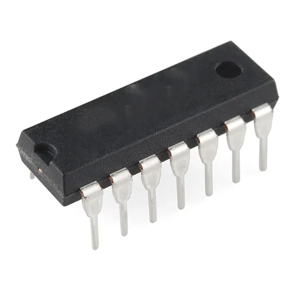
4013 IC Dual D-Type Flip-Flop
EGP 12
See other suppliers →Description
4013 IC Dual D-Type Flip-Flop The CD4013B is a monolithic integrated circuit fabricated using complementary MOS (CMOS) technology. It is designed as a dual, independent D-type flip-flop, meaning a single package contains two complete and separate data storage elements. Each flip-flop operates as a fundamental building block in digital electronics, capable of storing a single bit of data. The device is characterized by its high noise immunity and low power consumption, which are typical benefits of the CMOS construction process, making it suitable for a wide range of digital logic applications. Functionally, each flip-flop within the CD4013B features dedicated data (D), clock (CLK), set (SET), and reset (RESET) inputs, along for complementary outputs (Q and Q-not). The state of the D input is transferred to the Q output upon the application of a clock pulse, specifically on the positive-going edge. The independent Set and Reset inputs, which are active high, allow for the immediate setting or clearing of the flip-flop’s output regardless of the clock signal, providing direct control over the stored data state. This IC is offered in a variety of package options to accommodate different assembly and space requirements. These include 14-lead ceramic and plastic dual-in-line packages (CDIP, PDIP), as well as small-outline (SOIC) and thin shrink small-outline (TSSOP) packages for surface-mount technology. The CD4013B is specified for operation over a broad temperature range, supporting its use in industrial and military environments, and is part of the CD4000 series of logic chips which are known for their wide operating voltage range. Features: Constructed with CMOS technology for low power consumption and high noise immunity. Contains two independent, identical D-type flip-flops in one package. Features complementary Q and \Q outputs from each flip-flop. Includes asynchronous Set and Reset inputs for direct control. Positive-edge triggering on the clock input. Wide operating voltage range from 3V to 18V. High-voltage types (20V rating) for robust operation. Pinout Configurations: Pin No Pin Symbol Name Description 1,13 1Q/2Q Output Output Pin of the Flip Flop 2,12 1Q’(bar)/2Q’(bar) Complementary Output The inverted output pin of Flip Flop 3, 11 1CP/2CP Clock Input Pin These pins must be provided with a clock pulse for the flip-flop 4,10 1CD/2CD Clear Data Resets the flip-flop by clearing its memory 5,9 1D/2D Data Input Pin Input pin of the Flip Flop 6,8 1SD/2SD Set-direct Input Another Input pin for Flip Flop 7 Vss Ground Connected to the ground of the system 14 Vdd/Vcc Supply Voltage Powers the IC typically with 5V Specifications Parameter Condition Min Typ Max Unit Absolute Maximum Ratings DC Supply Voltage (VDD) – -0.5 – +20 V Input Voltage Range (All Inputs) – -0.5 – VDD + 0.5 V DC Input Current (Any One Input) – – – ±10 mA Power Dissipation (PD) TA = −55°C to +100°C – – 500 mW Operating Temperature Range (TA) – -55 – +125 °C Storage Temperature Range (Tstg) – -65 – +150 °C DC Electrical Characteristics Quiescent Device Current VDD = 20V, VO = 0/20V – 0.25 5.0 µA Input Capacitance (Cin) Any Input – 5.0 7.5 pF Dynamic Electrical Characteristics (TA = 25°C) Propagation Delay (Clock → Q) VDD = 5V – 150 300 ns VDD = 10V – 65 130 ns VDD = 15V – 45 90 ns Propagation Delay (Set/Reset → Q) VDD = 5V – 150 300 ns VDD = 10V – 65 130 ns VDD = 15V – 45 90 ns Maximum Clock Frequency (fCL) VDD = 5V 3.5 7 – MHz VDD = 10V 8 16 – MHz VDD = 15V 12 24 – MHz Minimum Clock Pulse Width (tw) VDD = 5V – 70 140 ns VDD = 10V – 30 60 ns VDD = 15V – 20 40 ns Minimum Set/Reset Pulse Width (tw) VDD = 5V – 90 180 ns VDD = 10V – 40 80 ns VDD = 15V – 25 50 ns Data Setup Time (ts) VDD = 5V – 20 40 ns VDD = 10V – 10 20 ns VDD = 15V – 7 15 ns Data Hold Time (th) VDD = 5V / 10V / 15V – 2 5 ns Clock Input Rise/Fall Time (tTLH, tTHL) VDD = 5V – – 15 µs VDD = 10V – – 10 µs VDD = 15V – – 5 µs Footprint Diagram: Applications: Used as Shift Registers. Memory/Control Registers. Buffer Circuits. Sampling Circuits. Latching devices. Package Contents: 1x 4013 IC Dual D-Type Flip-Flop Datasheet
From the supplier's page.
makhzan doesn't sell — every offer opens the supplier's own site.