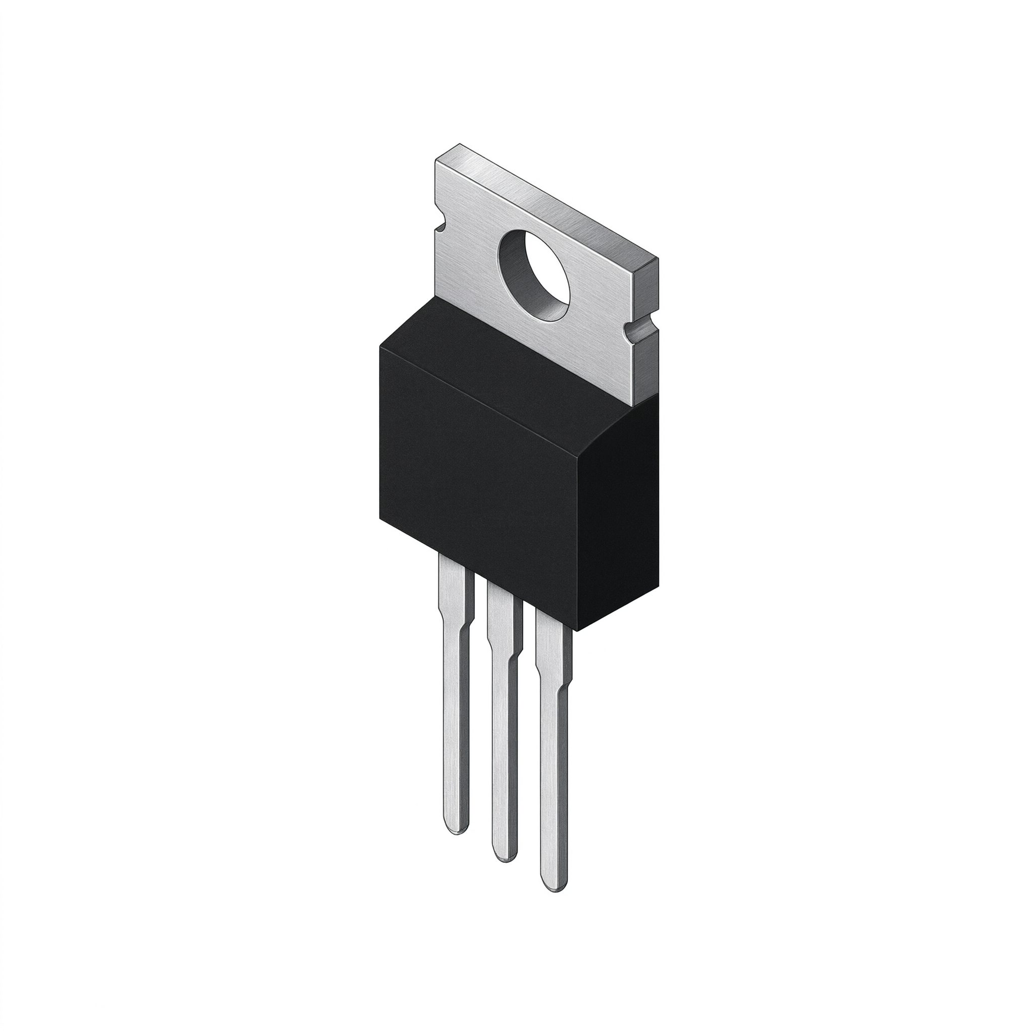
FQP13N80 N-Channel Power MOSFET 800V 12.6A TO-220
EGP 25
See other suppliers →Description
FQP13N80 N-Channel Power MOSFET 800V 12.6A TO-220 The FQP13N80 is a high-voltage, N-channel enhancement-mode power MOSFET built using Fairchild’s proprietary planar-stripe DMOS process (QFET technology). This design minimizes on-state resistance, delivers fast and efficient switching, and withstands high-energy pulses in avalanche and commutation modes — making the device exceptionally rugged in demanding power circuits. Features High voltage blocking: 800 V drain–source High current handling: 13 A continuous drain current (TC = 25 °C) Low on-state resistance: RDS(on) = 0.45 Ω max @ VGS = 10 V, ID = 6.5 A Low gate drive requirement — efficient switching with reduced drive loss Rugged avalanche and commutation (dv/dt) capability Integral body-drain diode Standard TO-220 package — easy mounting and heatsinking Max junction temperature: 150 °C Specifications General Part Number FQP13N80 Manufacturer Fairchild Semiconductor Device Type N-Channel Enhancement Mode Power MOSFET Package TO-220 Technology Proprietary planar stripe DMOS Absolute Maximum Ratings Drain-Source Voltage (VDSS) 800 V Continuous Drain Current (TC = 25°C) 12.6 A Continuous Drain Current (TC = 100°C) 8.0 A Pulsed Drain Current (IDM) 50.4 A Gate-Source Voltage (VGSS) ±30 V Single Pulsed Avalanche Energy (EAS) 1100 mJ Avalanche Current (IAR) 12.6 A Repetitive Avalanche Energy (EAR) 30 mJ Peak Diode Recovery dv/dt 4.0 V/ns Power Dissipation (TC = 25°C) 300 W Power Dissipation Derating Above 25°C 2.38 W/°C Operating and Storage Temperature Range -55 to +150 °C Maximum Lead Temperature 300 °C (1/8″ from case for 5 seconds) Thermal Characteristics Thermal Resistance, Junction-to-Case 0.42 °C/W (max) Thermal Resistance, Case-to-Sink 0.24 °C/W (typ) Thermal Resistance, Junction-to-Ambient 40 °C/W (max) Off Characteristics Drain-Source Breakdown Voltage (VGS = 0 V, ID = 250 µA) 800 V (min) Breakdown Voltage Temperature Coefficient (ID = 250 µA) 0.95 V/°C Zero Gate Voltage Drain Current (VDS = 800 V, VGS = 0 V) 10 µA (max) Zero Gate Voltage Drain Current (VDS = 640 V, TC = 125°C) 100 µA (max) Gate-Body Leakage Current, Forward (VGS = 30 V, VDS = 0 V) 100 nA (max) Gate-Body Leakage Current, Reverse (VGS = -30 V, VDS = 0 V) -100 nA (max) On Characteristics Gate Threshold Voltage (VDS = VGS, ID = 250 µA) 3.0 V to 5.0 V Static Drain-Source On-Resistance (VGS = 10 V, ID = 6.3 A) 0.58 Ω (typ), 0.75 Ω (max) Forward Transconductance (VDS = 50 V, ID = 6.3 A) 13 S (typ) Dynamic Characteristics (VDS = 25 V, VGS = 0 V, f = 1 MHz) Input Capacitance (Ciss) 2700 pF (typ), 3500 pF (max) Output Capacitance (Coss) 275 pF (typ), 360 pF (max) Reverse Transfer Capacitance (Crss) 30 pF (typ), 39 pF (max) Switching Characteristics (VDD = 400 V, ID = 12.6 A, RG = 25 Ω) Turn-On Delay Time (td(on)) 60 ns (typ), 130 ns (max) Turn-On Rise Time (tr) 150 ns (typ), 310 ns (max) Turn-Off Delay Time (td(off)) 155 ns (typ), 320 ns (max) Turn-Off Fall Time (tf) 110 ns (typ), 230 ns (max) Gate Charge (VDS = 640 V, ID = 12.6 A, VGS = 10 V) Total Gate Charge (Qg) 68 nC (typ), 88 nC (max) Gate-Source Charge (Qgs) 15 nC (typ) Gate-Drain Charge (Qgd) 32 nC (typ) Drain-Source Diode Characteristics Maximum Continuous Drain-Source Diode Forward Current (IS) 12.6 A Maximum Pulsed Drain-Source Diode Forward Current (ISM) 50.4 A Drain-Source Diode Forward Voltage (VGS = 0 V, IS = 12.6 A) 1.4 V (max) Reverse Recovery Time (trr) (VGS = 0 V, IS = 12.6 A, dIF/dt = 100 A/µs) 850 ns (typ) Reverse Recovery Charge (Qrr) 11.3 µC (typ) Applications High-Efficiency Switched-Mode Power Supplies (SMPS) Active Power Factor Correction (PFC) Circuits Electronic Lamp Ballasts (based on half-bridge topology) Package Content 1 x FQP13N80 N-Channel Power MOSFET 800V 12.6A TO-220 DataSheet FQA13N80-Fairchild
From the supplier's page.
makhzan doesn't sell — every offer opens the supplier's own site.