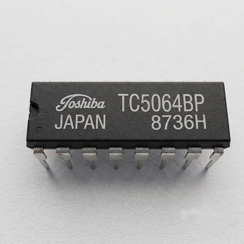
Toshiba TC5064BP Hex High-Voltage Buffer with Inhibit 3V to 18V 300mW DIP-16
EGP 75
See other suppliers →Description
Toshiba TC5064BP Hex High-Voltage Buffer with Inhibit 3V to 18V 300mW DIP-16 The TC5064BP is a C 2 MOS digital integrated circuit containing six non-inverting buffer circuits with open-drain structure outputs. It features two common INHIBIT inputs ( A IN , B IN ) and is built using high-breakdown-voltage P-channel MOS FETs capable of withstanding up to -50V. Designed for high-voltage output capabilities, the TC5064BP is an ideal solution for driving fluorescent display tubes and interfacing low-voltage logic with high-voltage MOS LSI circuits. Features Type: Hex High Voltage Buffer (Non-Inverting Type) High Output Voltage Capability: Features P-channel MOS FETs with open-drain structure capable of -50V breakdown voltage Control Inputs: Includes two common INHIBIT inputs ( A IN , B IN ) Output Impedance Control: Supports High-Impedance (HZ) state via INHIBIT pin configurations Wide Operating Voltage Range: 3V to 18V Package: 16-pin Dual In-line Package (DIP-16 / 3D16A-P) Specifications 1. Absolute Maximum Ratings ( T a = 25°C) Characteristic Symbol Rating Unit DC Supply Voltage V DD V SS – 0.5 ~ V SS + 20 V Input Voltage V IN V SS – 0.5 ~ V DD + 0.5 V Output Voltage V OUT V DD – 50 ~ V DD + 0.5 V Power Dissipation P D 300 mW DC Input Current I IN ±10 mA Storage Temperature Range T stg -65 ~ 150 °C Lead Temp. / Time T sol 260°C · 10sec — 2. Recommended Operating Conditions Characteristic Symbol Min. Typ. Max. Unit Supply Voltage V DD 3 — 18 V Input Voltage V IN 0 — V DD V Operating Temperature T opr -40 — 85 °C 3. Key Electrical Characteristics ( V SS = 0V) High Level Output Current ( I OH ): Up to -35mA (at V DD = 15V, V OH = 12V at 25°C) Output OFF Current ( I OFF ): -10µA max at V OUT = V DD – 45V (25°C) Quiescent Supply Current ( I DD ): 0.005µA (Typ. at V DD = 5V, 25°C) Input Capacitance ( C IN ): 5pF (Typ.), 7.5pF (Max) 4. Truth Table (TC5064BP) Input ( A IN ) Input ( B IN ) Input ( IN ) Output ( TC5064BP ) L H L HZ L H H H * L * HZ H * * HZ * HZ = High Impedance | * = Don’t care Applications Fluorescent Display Tube Driving Circuits: Driving digit and segment signals for VFDs. Logic Level Translation: Interfacing between CMOS/TTL/NMOS and PMOS circuits. High-Voltage MOS LSI Interfacing: Buffer stage driving for circuits operating with high negative voltages (e.g., -EV). Package Content 1 x Toshiba TC5064BP Hex High-Voltage Buffer with Inhibit 3V to 18V 300mW DIP-16 DataSheet TC5064BP
From the supplier's page.
makhzan doesn't sell — every offer opens the supplier's own site.