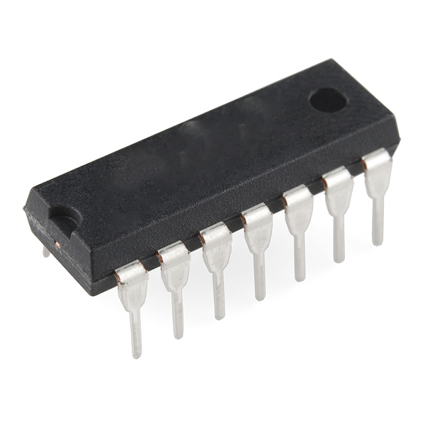
4069 CMOS Hex Inverter/NOT Gate 3V to 18V 1µA PDIP-14
EGP 13
See other suppliers →Description
CD4069BE CMOS Hex Inverter /NOT Gate 3V to 18V 1µA PDIP-14 The CD4069UB device consists of six CMOS inverter circuits. These devices are intended for all general-purpose inverter applications where the medium-power TTL-drive and logic-level-conversion capabilities of circuits such as the CD4009 and CD4049 hex inverter and buffers are not required. The CD4069UBE is supplied in a 14-pin PDIP package and operates from a recommended supply voltage range of 3 V to 18 V. It has standardized symmetrical output characteristics and medium-speed operation, with tPHL and tPLH of 30 ns typical at 10 V. The device is designed for applications including logic inversion, pulse shaping, oscillators, and high-input-impedance amplifiers. Its lower drive capability also makes it suitable for driving light loads such as LEDs and helps reduce the chance of overshoots and undershoots. Features Six CMOS inverter circuits in one package Standardized symmetrical output characteristics Wide recommended supply voltage range: 3 V to 18 V 100% tested for quiescent current at 20 V Maximum input current of 1 µA at 18 V over the full package-temperature range Recommended operating ambient temperature: -55°C to +125°C Specifications Function CMOS hex inverter Number of inverter circuits 6 Package PDIP-14, N package Body size 19.30 mm × 6.35 mm Pin count 14 Recommended supply voltage, VDD 3 V to 18 V Absolute maximum supply voltage, VDD -0.5 V to 20 V, stress rating only Input voltage, all inputs, absolute maximum -0.5 V to VDD + 0.5 V Recommended operating ambient temperature -55°C to +125°C Storage temperature -65°C to +150°C Input current 1 µA maximum at 18 V over full package-temperature range; 100 nA at 18 V and 25°C; static table limit ±1 µA maximum at VDD = 18 V Quiescent device current at 25°C 0.01 µA typical; 0.25 µA maximum at VDD = 5 V; 0.5 µA maximum at VDD = 10 V; 1 µA maximum at VDD = 15 V; 5 µA maximum at VDD = 20 V test condition Propagation delay time, tPLH/tPHL 30 ns typical at VDD = 10 V; 60 ns maximum at VDD = 10 V; 55 ns typical / 110 ns maximum at VDD = 5 V; 25 ns typical / 50 ns maximum at VDD = 15 V Transition time, tTHL/tTLH 50 ns typical / 100 ns maximum at VDD = 10 V; 100 ns typical / 200 ns maximum at VDD = 5 V; 40 ns typical / 80 ns maximum at VDD = 15 V Input capacitance 10 pF typical, 15 pF maximum Low-level output voltage, VOL 0.05 V maximum at VDD = 5 V, 10 V, or 15 V High-level output voltage, VOH 4.95 V minimum at VDD = 5 V; 9.95 V minimum at VDD = 10 V; 14.95 V minimum at VDD = 15 V Input low voltage, VIL 1 V maximum at VDD = 5 V; 2 V maximum at VDD = 10 V; 2.5 V maximum at VDD = 15 V Input high voltage, VIH 4 V minimum at VDD = 5 V; 8 V minimum at VDD = 10 V; 12.5 V minimum at VDD = 15 V Output low sink current, IOL VDD = 5 V: 0.51 mA minimum / 1 mA typical; VDD = 10 V: 1.3 mA minimum / 2.6 mA typical; VDD = 15 V: 3.4 mA minimum / 6.8 mA typical Output high source current, IOH VDD = 5 V: -0.51 mA minimum / -1 mA typical; VDD = 10 V: -1.3 mA minimum / -2.6 mA typical; VDD = 15 V: -3.4 mA minimum / -6.8 mA typical Absolute maximum DC input current, any one input -10 mA to +10 mA Power dissipation 500 mW per package from -55°C to 100°C; 100 mW per output transistor Junction temperature 150°C maximum Lead temperature 265°C maximum Applications Logic inversion Pulse shaping Oscillators High-input-impedance amplifiers Package Content 1 x CD4069BE CMOS Hex Inverter/NOT Gate 3V to 18V 1µA PDIP-14 DataSheet cd4069ub
From the supplier's page.
makhzan doesn't sell — every offer opens the supplier's own site.