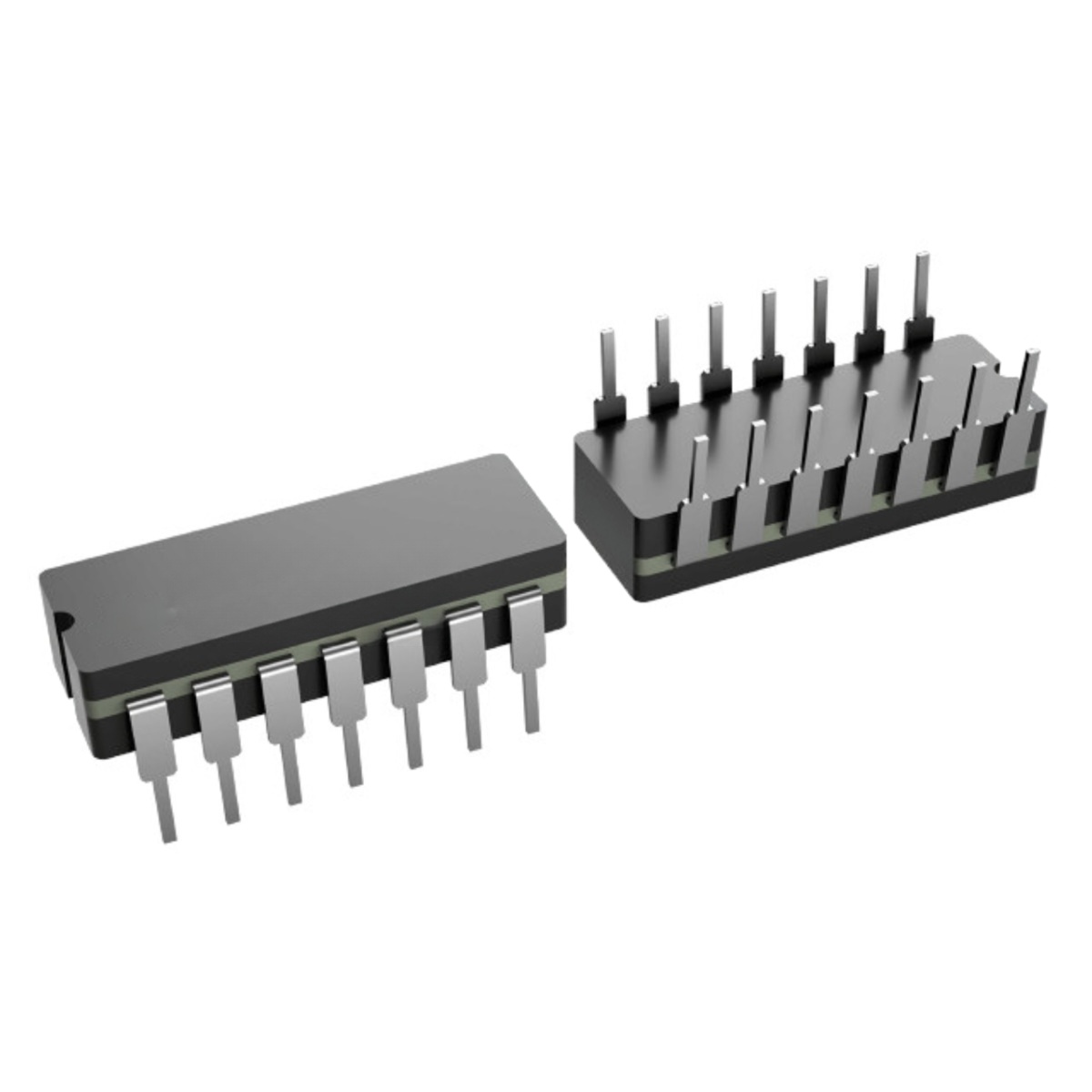
CD4011B High-Voltage CMOS Quad 2-Input NAND Gate 20V ±10mA DIP-14
Part number CD4011B
From the shop's description
CD4011B High-Voltage CMOS Quad 2-Input NAND Gate 20V ±10mA DIP-14 The CD4011B is a high-voltage CMOS integrated circuit containing four independent 2-input NAND gates. It provides system designers with a direct implementation of the NAND logic function and supplements the existing family of CMOS gates. To ensure exceptional signal consistency, uniform driving capability, and noise immunity across various operational states, all inputs and outputs are fully buffered. Features: Buffered Inputs and Outputs. High-Voltage Types. Standardized Symmetrical Output. Ultra-Low Quiescent Current. High Noise Margin. Industry Standards Compliance. Specifications: Category Parameter / Characteristic Test Conditions / Details Value / Range Units Recommended Operating Conditions Operating Supply: Supply-Voltage Range (VDD) Over full package temperature range 3 to 18 V Temperature: Operating Temperature Range (TA) – -55 to +125 °C Absolute Maximum Ratings Absolute Ratings: DC Supply-Voltage Range (VDD) Voltages referenced to VSS terminal -0.5 to +20 V Input Voltage Range All inputs -0.5 to VDD + 0.5 V DC Input Current Any one input ±10 mA Power Dissipation Per Package (PD) For TA = -55°C to +100°C (Derate linearly at 12mW/°C to 200mW from +100°C to +125°C) 500 mW Device Dissipation Per Output Transistor Over full package temperature range 100 mW Dynamic Electrical Characteristics (at TA = 25°C, CL = 50 pF, RL = 200 kΩ, Input tr, tf = 20 ns) Propagation Delay Time: tPHL, tPLH (Typical / Maximum) VDD = 5 V 125 / 250 ns VDD = 10 V 60 / 120 ns VDD = 15 V 45 / 90 ns Transition Time: tTHL, tTLH (Typical / Maximum) VDD = 5 V 100 / 200 ns VDD = 10 V 50 / 100 ns VDD = 15 V 40 / 80 ns Capacitance: Input Capacitance (CIN) Any input (Typical / Maximum) 5 / 7.5 pF Thermal & Soldering Specifications Storage & Soldering: Storage Temperature Range (Tstg) – -65 to +150 °C Lead Temperature (During Soldering) Distance 1/16 ± 1/32 inch (1.59 ± 0.79mm) from case for 10s max +265 (Max) °C All measurements are shown in Inches with Millimeters provided in brackets Applications: Direct implementation of the NAND logic function. Gating networks and custom logic circuits. Signal squaring and buffering pipelines in standard/high-voltage CMOS systems. Package Content: 1x CD4011B High-Voltage CMOS Quad 2-Input NAND Gate 20V ±10mA DIP-14 Datasheet CD4011B
Read moreShow less
Similar products
 74HC02 (Quad 2-Input NOR Gate)EGP 10 – 153 shopschecked 13 days ago
 ULN2003A, 7-element NPN Darlington Pair 500mA 50VEGP 101 shopchecked 15 days ago
 MOC 3011 Optoisolator Triac DriverEGP 101 shopchecked 20 days ago
 74HC00 – 7400 ( Quad 2-Input NAND Gate )EGP 10 – 153 shopschecked 16 days ago
 74LS11 Triple 3-Input AND Gate DIP-14EGP 10 – 202 shopschecked 11 days ago
 Battery Level Indicator IC KA2284 9-PinEGP 101 shopchecked 12 days ago
 L9110 Dual Motor Driver ICEGP 101 shopchecked 27 days ago
- 4001 IC Quad 2-Input NOR Gate DIP-14EGP 101 shopchecked 20 days ago